

扫一扫
关注中图网
官方微博


本类五星书更多>
-
>
公路车宝典(ZINN的公路车维修与保养秘籍)

-
>
晶体管电路设计(下)
-
>
基于个性化设计策略的智能交通系统关键技术
-
>
花样百出:贵州少数民族图案填色
-
>
山东教育出版社有限公司技术转移与技术创新历史丛书中国高等技术教育的苏化(1949—1961)以北京地区为中心
-
>
铁路机车概要.交流传动内燃.电力机车
-
>
利维坦的道德困境:早期现代政治哲学的问题与脉络
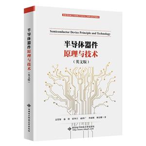
半导体器件原理与技术 版权信息
- ISBN:9787560666204
- 条形码:9787560666204 ; 978-7-5606-6620-4
- 装帧:一般胶版纸
- 册数:暂无
- 重量:暂无
- 所属分类:>>
半导体器件原理与技术 内容简介
This book comprehensively and deeply introduces the semiconductor device principle and technology. The book consists of three sections: semiconductor physics and devices, semiconductor manufacturing process and semiconductor packaging,testing and simulating. The first section mainly introduces semiconductor physics foundation, diode, bipolar junction transistor, MOS field effect transistor, power MOSFET, thyristor, IGBT, passive device and SPICE model. The second section mainly introduces semiconductor process technology, semiconductor process simulation and film preparation technology. The third section mainly introduces semiconductor packaging, testing and simulating technology. These contents will lay a solid foundation for further mastering the basic theories and methods of analysis, design, manufacturing, packaging and testing of semiconductor devices. This book can be used as a textbook for undergraduate and graduate students who are engaged in the analysis, design, manufacturing, packaging and testing of semiconductor devices and IC design. It can also be used as a selfstudy and reference book for professional engineers.
半导体器件原理与技术 目录
SECTION Ⅰ Semiconductor Physics and Devices
Chapter 1 Semiconductor physics foundation 3
1.1 Semiconductor materials 3
1.2 Semiconductor structure 6
1.3 Semiconductor defects 10
1.4 Energy band of semiconductor 14
1.5 Fermi level 18
1.6 Carrier concentration of semiconductor 20
1.7 Carrier motion of semiconductor 25
1.7.1 Carrier drift 25
1.7.2 Carrier diffusion 26
1.7.3 Carrier recombination 28
Exercises 30
References 31
Chapter 2 Diode 33
2.1 Basic structure of diode 33
2.2 Formation of pn junction and impurity distribution 35
2.3 Equilibrium pn junction 36
2.3.1 Formation of space charge region 36
2.3.2 Energy band of pn junction 38
2.3.3 Contact potential difference 39
2.3.4 Space charge region characteristics 40
2.3.5 Electric field and width of space charge region 41
2.4 Bias characteristics of diodes 44
2.4.1 Forward bias 44
2.4.2 Reverse bias 46
2.5 Influencing factors of diode DC characteristics 48
2.5.1 Recombination current and generation current in space charge region 49
2.5.2 Surface effect 49
2.5.3 Series resistance effect 49
2.5.4 Large injection effect 50
2.5.5 Temperature effect 50
2.6 Breakdown characteristics of diode 50
2.6.1 Avalanche breakdown 51
2.6.2 Tunnel breakdown 51
2.6.3 Thermoelectric breakdown 52
2.7 Switching characteristics of diode 52
Exercises 54
References 57
Chapter 3 Bipolar junction transistor 59
3.1 Introduction of BJT 59
3.2 Basic architecture of bipolar transistor 60
3.2.1 Alloy transistor 61
3.2.2 Alloy diffusion transistor 62
3.2.3 Planar transistor 63
3.2.4 Mesa transistor 63
3.3 Amplification of bipolar junction transistor 64
3.3.1 Carrier transmisson characteristics 65
3.3.2 Current amplification coefficient 68
3.3.3 Amplification conditions 70
3.4 Characteristic curve of bipolar transistor 71
3.4.1 Common base characteristic curve 71
3.4.2 Common emitter characteristic curve 73
3.5 Reverse current and breakdown voltage characteristics 76
3.5.1 Reverse current 76
3.5.2 Breakdown voltage 78
3.6 Base resistance 81
3.6.1 Concept of base resistance 81
3.6.2 Base resistance of comb transistor 82
3.6.3 Base resistance of circular transistor 83
3.7 Switching characteristics of bipolar junction transistor 84
3.7.1 On state and off state 84
3.7.2 Transient switching characteristics 85
Exercises 87
References 89
Chapter 4 MOS field effect transistor 91
4.1 Basic structure, principle and classification of MOSFET 91
4.1.1 Basic structure of MOSFET 92
4.1.2 Operating principle of MOSFET 92
4.1.3 Classification of MOSFET 93
4.2 Threshold voltage of MOSFET 96
4.2.1 Charge distribution in MOS structure 96
4.2.2 Threshold voltage of ideal MOSFET 98
4.2.3 Threshold voltage of actual MOSFET 98
4.3 DC characteristics of MOSFET 99
4.3.1 Operating characteristics of MOSFET 100
4.3.2 Breakdown characteristics of MOSFET 104
4.4 Small signal parameters and frequency characteristics of MOSFET 108
4.4.1 Small signal parameters of MOSFET 109
4.4.2 Frequency characteristics of MOSFET 112
4.5 Secondorder effects of MOSFET 115
4.5.1 Nonconstant mobility effect 115
4.5.2 Bulk charge effect 116
4.5.3 Short channel effect 119
4.5.4 Narrow channel effect 121
4.6 Switching characteristics of MOSFET 122
4.6.1 Transient switching delay 123
4.6.2 Calculation of switching time 124
Exercises 126
References 128
Chapter 5 Power MOSFET 130
5.1 Introduction 130
5.2 Structure of power MOSFET devices 131
5.3 Channel characteristics 133
5.4 Conduction loss 135
5.5 Switching characteristics 137
5.6 Selection of power MOSFET devices 141
Exercises 143
References 145
Chapter 6 Thyristor 147
6.1 Introduction 147
6.2 Device structure and working principle 148
6.3 IV characteristics of thyristor 151
6.3.1 Static characteristics 151
6.3.2 Dynamic characteristics 152
6.4 Conduction characteristics 153
6.5 Shutdown characteristics 156
6.5.1 Interrupt anode current 157
6.5.2 Reverse voltage interruption 158
Exercises 160
References 162
Chapter 7 IGBT 163
7.1 Introduction 163
7.2 Device structure and working mechanism of IGBT 165
7.3 IV characteristics of IGBT 167
7.4 Switching characteristics of IGBT 168
7.4.1 Conduction characteristics 168
7.4.2 Shutdown characteristics 170
Exercises 172
References 173
Chapter 8 Passive devices 174
8.1 Introduction 174
8.2 Embedded passive devices 176
8.3 Integrated passive devices 176
8.4 Integrated resistance 178
8.4.1 Bipolar transistor processing resistance 178
8.4.2 CMOS processing resistance 182
8.4.3 Resistance value calculation and common graphics 183
8.4.4 Resistance parasitic effect 185
8.5 Integrated capacitance 188
8.5.1 Type of integrated capacitance 188
8.5.2 Capacitance parasitic effect 192
8.6 Integrated inductance 195
8.6.1 Integrated inductance structure 195
8.6.2 Inductive parasitic effect 196
Exercises 198
References 201
Chapter 9 SPICE device model 202
9.1 Introduction 202
9.2 Diode SPICE model 205
9.2.1 DC model of diode 205
9.2.2 Transient model of diode 206
9.2.3 AC model of diode 206
9.2.4 Noise model of diode 207
9.2.5 Temperature effect of diode 207
9.3 SPICE model of bipolar transistor 209
9.3.1 Small signal model of bipolar transistor 209
9.3.2 Transient analysis 209
9.3.3 Noise analysis 212
9.3.4 Temperature effect 214
9.4 SPICE model of MOS field effect transistor 216
9.4.1 Small signal model of MOSFET 216
9.4.2 Noise model of MOSFET 218
9.4.3 Transient model of MOSFET 218
9.4.4 Temperature effect of MOSFET 220
9.4.5 Second order effect and higher order effect models 221
9.5 SPICE model of passive devices 224
9.5.1 Resistance 224
9.5.2 Capacitance 225
9.5.3 Inductance 226
Exercises 226
References 228
SECTION Ⅱ Semiconductor Manufacturing Process
Chapter 10 Semiconductor process technology 231
10.1 Substrate cleaning 232
10.1.1 Wet chemical cleaning 233
10.1.2 Dry cleaning 234
10.1.3 Beam cleaning 235
10.2 Oxidation technology 235
10.2.1 Structure and properties of SiO2 film 235
10.2.2 Thermal oxidation 239
10.2.3 Quality analysis of oxide layer 243
10.2.4 Other oxidation methods 246
10.3 Graphic processing technology 247
10.3.1 Photo etching process flow 248
10.3.2 Photoresist classification 249
10.3.3 Mask preparation 250
10.3.4 Photolithography technology 252
10.3.5 Etching technology 255
10.3.6 Defect analysis 258
10.4 Doping technology 261
10.4.1 Basic concept of doping 261
10.4.2 Thermal diffusion 261
10.4.3 Ion implantation 267
10.4.4 Other doping methods 272
Exercises 272
References 275
Chapter 11 Semiconductor process simulation 276
11.1 Introduction 276
11.1.1 Program startup 277
11.1.2 Example loading 277
11.2 nchannel MOSFET simulation 278
11.2.1 Simulation grid construction 279
11.2.2 Substrate initialization 281
11.2.3 ATHENA operation and drawing 282
11.2.4 Gate oxidation process 283
11.2.5 Ion implantation 288
11.2.6 Polysilicon gate deposition 291
11.2.7 Polysilicon etching 292
11.2.8 Polysilicon oxidation 294
11.2.9 Polysilicon doping 295
11.2.10 Isolated oxide deposition 297
11.2.11 Isolation oxide etching 297
11.2.12 Source/Drain injection and annealing 298
11.2.13 Metal deposition 299
11.2.14 Extraction of device parameters 302
11.2.15 Half nchannel MOS structure image 303
11.2.16 Electrode marking 304
11.2.17 Save ATHENA structure file 305
11.3 Lithography process simulation 306
11.3.1 Mask design 306
11.3.2 Light source selection 308
11.3.3 Parameter configuration of projection system 308
11.3.4 Filter parameter configuration 309
11.3.5 Imaging 309
11.3.6 Exposure 310
11.3.7 Baking 311
11.3.8 Development 311
11.3.9 Complete lithography process 312
Exercises 314
References 315
Chapter 12 Film preparation technology 316
12.1 Physical preparation technology 317
12.1.1 Vacuum foundation 317
12.1.2 Vacuum evaporation coating 326
12.1.3 Sputtering coating 329
12.1.4 Molecular beam epitaxy 334
12.1.5 Pulsed laser deposition 338
12.2 Chemical preparation technology 342
12.2.1 Chemical vapor deposition 343
12.2.2 Chemical solution preparation 352
12.2.3 Soft solution processing 358
Exercises 360
References 363
SECTION Ⅲ Semiconductor Packaging, Testing and Simulating
Chapter 13 Semiconductor packaging technology 367
13.1 Introduction 367
13.2 Packaging function 369
13.2.1 Physical protection 369
13.2.2 Electrical connection 369
13.2.3 Heat dissipation 370
13.3 Packaging process 371
13.3.1 Overview of process flow 371
13.3.2 Chip mounting 372
13.3.3 Chip interconnection 374
13.3.4 Molding technology 378
13.4 Packaging materials 379
13.4.1 Molding materials 379
13.4.2 Frame materials 381
13.5 Packaging type 383
13.5.1 Pin 383
13.5.2 Surface Mount 385
13.5.3 Array 388
13.6 Other packaging technologies 390
13.6.1 Multichip packaging 390
13.6.2 Chip level packaging 392
13.6.3 Preencapsulated interconnection system 393
13.6.4 Flip chip packaging 394
Exercises 396
References 398
Chapter 14 Semiconductor parameter testing technology 400
14.1 Semiconductor resistivity testing 400
14.1.1 Introduction 400
14.1.2 Fourpoint probe testing method 402
14.1.3 Influencing factors 407
14.2 Conductivity type testing of semiconductor 408
14.2.1 Hot and cold probe method 408
14.2.2 Single probe point contact rectification method 409
14.2.3 Influencing factors 412
14.3 Oxide film thickness testing 413
14.3.1 Color contrast method 413
14.3.2 Optical interferometry 414
14.3.3 High frequency turbulence method 415
14.3.4 Ellipsometry 416
14.4 Junction depth testing 417
14.5 Testing of impurity concentration of epitaxial layer 418
14.6 Testing of nonequilibrium minority carrier lifetime 421
14.6.1 Overview 421
14.6.2 Lifetime of nonequilibrium minority carriers 422
14.6.3 Testing method 422
14.7 Bipolar transistor parameter testing 424
14.7.1 DC parameter testing 424
14.7.2 Testing of Ccr′bb product 426
14.7.3 Testing of switching parameters 427
14.7.4 Characteristic frequency testing 429
14.7.5 Steadystate thermal resistance testing 433
14.8 MOSFET parameter testing 435
14.8.1 DC characteristic testing 435
14.8.2 Testing of input capacitance and feedback capacitance 437
14.8.3 Testing of power gain and noise coefficient 438
Exercises 440
References 443
Chapter 15 Realization technology of semiconductor device characteristic simulation based on GUI 445
15.1 Introduction 445
15.2 Software architecture design 446
15.3 Project creation 448
15.4 Main page design 453
15.5 Semiconductor physical parameters 457
15.5.1 Fermi potential calculation 457
15.5.2 Carrier concentration calculation 460
15.5.3 Energy level calculation of single hydrogen atom 462
15.6 Semiconductor device parameters 463
15.6.1 CMOS device characteristics 463
15.6.2 Resistivity calculation 468
15.6.3 Junction depth calculation 470
15.6.4 Calculation of oxide film thickness 472
15.6.5 Contact potential difference calculation 473
15.7 Multimedia resources 475
15.8 Accessibility functions 479
15.9 Help file design 481
Exercises 483
References 484
Appendix 485
Keys to exercises 495
展开全部
书友推荐
- >
我与地坛
我与地坛
¥16.4¥28.0 - >
莉莉和章鱼
莉莉和章鱼
¥14.4¥42.0 - >
中国历史的瞬间
中国历史的瞬间
¥16.7¥38.0 - >
姑妈的宝刀
姑妈的宝刀
¥15.7¥30.0 - >
大红狗在马戏团-大红狗克里弗-助人
大红狗在马戏团-大红狗克里弗-助人
¥5.2¥10.0 - >
罗曼·罗兰读书随笔-精装
罗曼·罗兰读书随笔-精装
¥32.9¥58.0 - >
龙榆生:词曲概论/大家小书
龙榆生:词曲概论/大家小书
¥8.7¥24.0 - >
有舍有得是人生
有舍有得是人生
¥25.7¥45.0
本类畅销
-

电机与电气控制技术
¥27.9¥49 -
电工电子技术及应用(第2版)
¥20.5¥39.8 -
通信原理简明教程
¥10.8¥28 -
电子产品工艺
¥23.4¥66 -
配电实用技术 第4版
¥65.3¥99 -
新能源科学与工程应用丛书光伏发电原理.技术及其应用
¥45.9¥69
浏览历史
复张量优化及其在量子信息中的应用
¥59.5¥78.0光学基本原理
¥62.7¥98.0数字通信
¥18.3¥24.0带有通配符和长度约束的模式匹配
¥77.4¥98.0工程设计制图(第二版)
¥32.4¥49.8