-
>
中医基础理论
-
>
高校军事课教程
-
>
思想道德与法治(2021年版)
-
>
毛泽东思想和中国特色社会主义理论体系概论(2021年版)
-
>
中医内科学·全国中医药行业高等教育“十四五”规划教材
-
>
中医诊断学--新世纪第五版
-
>
中药学·全国中医药行业高等教育“十四五”规划教材
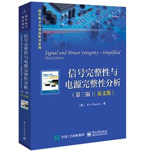
信号完整性与电源完整性分析(第三版)(英文版)(本科教材) 版权信息
- ISBN:9787121407833
- 条形码:9787121407833 ; 978-7-121-40783-3
- 装帧:一般胶版纸
- 册数:暂无
- 重量:暂无
- 所属分类:>>
信号完整性与电源完整性分析(第三版)(英文版)(本科教材) 本书特色
适读人群 :本书是面向电子行业设计工程师和产品负责人的一本具有实用价值的参考书,研读此书有助于在信号与电源完整性问题出现之前提前发现并及早加以解决。同时,本书也可作为相关专业本科生及研究生的双语教学用书。本书全面论述了信号完整性与电源完整性问题。主要讲述信号与电源完整性分析及物理设计概论,4类信号与电源完整性问题的实质含义,物理互连设计对信号完整性的影响,电容、电感、电阻和电导的特性分析,求解信号与电源完整性问题的4种实用技术途径,推导和仿真背后隐藏的解决方案,以及改进信号与电源完整性的推荐设计准则等。本书还讨论了信号与电源完整性中S参数的应用问题,并给出了电源分配网络的设计实例。
信号完整性与电源完整性分析(第三版)(英文版)(本科教材) 内容简介
本书全面论述了信号完整性与电源完整性问题。主要讲述信号与电源完整性分析及物理设计概论,4类信号与电源完整性问题的实质含义,物理互连设计对信号完整性的影响,电容、电感、电阻和电导的特性分析,求解信号与电源完整性问题的4种实用技术途径,推导和仿真背后隐藏的解决方案,以及改进信号与电源完整性的推荐设计准则等。本书还讨论了信号与电源完整性中S参数的应用问题,并给出了电源分配网络的设计实例。本书强调直觉理解、实用工具和工程素养。作者以实践专家的视角指出造成信号与电源完整性问题的根源,并特别给出了设计阶段前期的问题解决方案。
信号完整性与电源完整性分析(第三版)(英文版)(本科教材) 目录
1.1 What Are Signal Integrity, Power Integrity, and Electromagnetic Compatibility?
1.2 Signal-Integrity Effects on One Net
1.3 Cross Talk
1.4 Rail-Collapse Noise
1.5 ElectroMagnetic Interference (EMI)
1.6 Two Important Signal-Integrity Generalizations
1.7 Trends in Electronic Products
1.8 The Need for a New Design Methodology
1.9 A New Product Design Methodology
1.10 Simulations
1.11 Modeling and Models
1.12 Creating Circuit Models from Calculation
1.13 Three Types of Measurements
1.14 The Role of Measurements
1.15 The Bottom Line
Chapter 2 Time and Frequency Domains
2.1 The Time Domain
2.2 Sine Waves in the Frequency Domain
2.3 Shorter Time to a Solution in the Frequency Domain
2.4 Sine-Wave Features
2.5 The Fourier Transform
2.6 The Spectrum of a Repetitive Signal
2.7 The Spectrum of an Ideal Square Wave
2.8 From the Frequency Domain to the Time Domain
2.9 Effect of Bandwidth on Rise Time
2.10 Bandwidth and Rise Time
2.11 What Does Significant Mean?
2.12 Bandwidth of Real Signals
2.13 Bandwidth and Clock Frequency
2.14 Bandwidth of a Measurement
2.15 Bandwidth of a Model
2.16 Bandwidth of an Interconnect
2.17 The Bottom Line
Chapter 3 Impedance and Electrical Models
3.1 Describing Signal-Integrity Solutions in Terms of Impedance
3.2 What Is Impedance?
3.3 Real Versus Ideal Circuit Elements
3.4 Impedance of an Ideal Resistor in the Time Domain
3.5 Impedance of an Ideal Capacitor in the Time Domain
3.6 Impedance of an Ideal Inductor in the Time Domain
3.7 Impedance in the Frequency Domain
3.8 Equivalent Electrical Circuit Models
3.9 Circuit Theory and SPICE
3.10 Introduction to Measurement-Based Modeling
3.11 The Bottom Line
Chapter 4 The Physical Basis of Resistance
4.1 Translating Physical Design into Electrical Performance
4.2 The Only Good Approximation for the Resistance of Interconnects
4.3 Bulk Resistivity
4.4 Resistance per Length
4.5 Sheet Resistance
4.6 The Bottom Line
Chapter 5 The Physical Basis of Capacitance
5.1 Current Flow in Capacitors
5.2 The Capacitance of a Sphere
5.3 Parallel Plate Approximation
5.4 Dielectric Constant
5.5 Power and Ground Planes and Decoupling Capacitance
5.6 Capacitance per Length
5.7 2D Field Solvers
5.8 Effective Dielectric Constant
5.9 The Bottom Line
Chapter 6 The Physical Basis of Inductance
6.1 What Is Inductance?
6.2 Inductance Principle 1: There Are Circular Rings of Magnetic-Field Lines Around All Currents
6.3 Inductance Principle 2: Inductance Is the Number of Webers of Field Line Rings Around a Conductor per Amp of Current Through It
6.4 Self-Inductance and Mutual Inductance
6.5 Inductance Principle 3: When the Number of Field Line Rings Around a Conductor Changes, There Will Be a Voltage Induced Across the Ends of the Conductor
6.6 Partial Inductance
6.7 Effective, Total, or Net Inductance and Ground Bounce
6.8 Loop Self- and Mutual Inductance
6.9 The Power Distribution Network (PDN) and Loop Inductance
6.10 Loop Inductance per Square of Planes
6.11 Loop Inductance of Planes and Via Contacts
6.12 Loop Inductance of Planes with a Field of Clearance Holes
6.13 Loop Mutual Inductance
6.14 Equivalent Inductance of Multiple Inductors
6.15 Summary of Inductance
6.16 Current Distributions and Skin Depth
6.17 High-Permeability Materials
6.18 Eddy Currents
6.19 The Bottom Line
Chapter 7 The Physical Basis of Transmission Lines
7.1 Forget the Word Ground
7.2 The Signal
7.3 Uniform Transmission Lines
7.4 The Speed of Electrons in Copper
7.5 The Speed of a Signal in a Transmission Line
7.6 Spatial Extent of the Leading Edge
7.7 “Be the Signal”
7.8 The Instantaneous Impedance of a Transmission Line
7.9 Characteristic Impedance and Controlled Impedance
7.10 Famous Characteristic Impedances
7.11 The Impedance of a Transmission Line
7.12 Driving a Transmission Line
7.13 Return Paths
7.14 When Return Paths Switch Reference Planes
7.15 A First-Order Model of a Transmission Line
7.16 Calculating Characteristic Impedance with Approximations
7.17 Calculating the Characteristic Impedance with a 2D Field Solver
7.18 An n-Section Lumped-Circuit Model
7.19 Frequency Variation of the Characteristic Impedance
7.20 The Bottom Line
Chapter 8 Transmission Lines and Reflections
8.1 Reflections at Impedance Changes
8.2 Why Are There Reflections?
8.3 Reflections from Resistive Loads
8.4 Source Impedance
8.5 Bounce Diagrams
8.6 Simulating Reflected Waveforms
8.7 Measuring Reflections with a TDR
8.8 Transmission Lines and Unintentional Discontinuities
8.9 When to Terminate
8.10 The Most Common Termination Strategy for Point-to-Point Topology
8.11 Reflections from Short Series Transmission Lines
8.12 Reflections from Short-Stub Transmission Lines
8.13 Reflections from Capacitive End Terminations
8.14 Reflections from Capacitive Loads in the Middle of a Trace
8.15 Capacitive Delay Adders
8.16 Effects of Corners and Vias
8.17 Loaded Lines
8.18 Reflections from Inductive Discontinuities
8.19 Compensation
8.20 The Bottom Line
Chapter 9 Lossy Lines, Rise-Time Degradation, and Material Properties
9.1 Why Worry About Lossy Lines?
9.2 Losses in Transmission Lines
9.3 Sources of Loss: Conductor Resistance and Skin Depth
9.4 Sources of Loss: The Dielectric
9.5 Dissipation Factor
9.6 The Real Meaning of Dissipation Factor
9.7 Modeling Lossy Transmission Lines
9.8 Characteristic Impedance of a Lossy Transmission Line
9.9 Signal Velocity in a Lossy Transmission Line
9.10 Attenuation and dB
9.11 Attenuation in Lossy Lines
9.12 Measured Properties of a Lossy Line in the Frequency Domain
9.13 The Bandwidth of an Interconnect
9.14 Time-Domain Behavior of Lossy Lines
9.15 Improving the Eye Diagram of a Transmission Line
9.16 How Much Attenuation Is Too Much?
9.17 The Bottom Line
Chapter 10 Cross Talk in Transmission Lines
10.1 Superposition
10.2 Origin of Coupling: Capacitance and Inductance
10.3 Cross Talk in Transmission Lines: NEXT and FEXT
10.4 Describing Cross Talk
10.5 The SPICE Capacitance Matrix
10.6 The Maxwell Capacitance Matrix and 2D Field Solvers
10.7 The Inductance Matrix
10.8 Cross Talk in Uniform Transmission Lines and Saturation Length
10.9 Capacitively Coupled Currents
10.10 Inductively Coupled Currents
10.11 Near-End Cross Talk
10.12 Far-End Cross Talk
10.13 Decreasing Far-End Cross Talk
10.14 Simulating Cross Talk
10.15 Guard Traces
10.16 Cross Talk and Dielectric Constant
10.17 Cross Talk and Timing
10.18 Switching Noise
10.19 Summary of Reducing Cross Talk
10.20 The Bottom Line
Chapter 11 Differential Pairs and Differential Impedance
11.1 Differential Signaling
11.2 A Differential Pair
11.3 Differential Impedance with No Coupling
11.4 The Impact from Coupling
11.5 Calculating Differential Impedance
11.6 The Return-Current Distribution in a Differential Pair
11.7 Odd and Even Modes
11.8 Differential Impedance and Odd-Mode Impedance
11.9 Common Impedance and Even-Mode Impedance
11.10 Differential and Common Signals and Odd- and Even-Mode Voltage Components
11.11 Velocity of Each Mode and Far-End Cross Talk
11.12 Ideal Coupled Transmission-Line Model or an Ideal Differential Pair
11.13 Measuring Even- and Odd-Mode Impedance
11.14 Terminating Differential and Common Signals
11.15 Conversion of Differential to Common Signals
11.16 EMI and Common Signals
11.17 Cross Talk in Differential Pairs
11.18 Crossing a Gap in the Return Path
11.19 To Tightly Couple or Not to Tightly Couple
11.20 Calculating Odd and Even Modes from Capacitance- and Inductance-Matrix Elements
11.21 The Impedance Matrix
11.22 The Bottom Line
Chapter 12 S-Parameters for Signal-Integrity Applications
12.1 S-Parameters, the New Universal Metric
12.2 What Are S-Parameters?
12.3 Basic S-Parameter Formalism
12.4 S-Parameter Matrix Elements
12.5 Introducing the Return and Insertion Loss
12.6 A Transparent Interconnect
12.7 Changing the Port Impedance
12.8 The Phase of S21 for a Uniform 50-Ohm Transmission Line
12.9 The Magnitude of S21 for a Uniform Transmission Line
12.10 Coupling to Other Transmission Lines
12.11 Insertion Loss for Non-50-Ohm Transmission Lines
12.12 Data-Mining S-Parameters
12.13 Single-Ended and Differential S-Parameters
12.14 Differential Insertion Loss
12.15 The Mode Conversion Terms
12.16 Converting to Mixed-Mode S-Parameters
12.17 Time and Frequency Domains
12.18 The Bottom Line
Chapter 13 The Power Distribution Network (PDN)
13.1 The Problem
13.2 The Root Cause
13.3 The Most Important Design Guidelines for the PDN
13.4 Establishing the Target Impedance Is Hard
13.5 Every Product Has a Unique PDN Requirement
13.6 Engineering the PDN
13.7 The VRM
13.8 Simulating Impedance with SPICE
13.9 On-Die Capacitance
13.10 The Package Barrier
13.11 The PDN with No Decoupling Capacitors
13.12 The MLCC Capacitor
13.13 The Equivalent Series Inductance
13.14 Approximating Loop Inductance
13.15 Optimizing the Mounting of Capacitors
13.16 Combining Capacitors in Parallel
13.17 Engineering a Reduced Parallel Resonant Peak by Adding More Capacitors
13.18 Selecting Capacitor Values
13.19 Estimating the Number of Capacitors Needed
13.20 How Much Does a nH Cost?
13.21 Quantity or Specific Values?
13.22 Sculpting the Impedance Profiles: The Frequency-Domain Target Impedance Method (FDTIM)
13.23 When Every pH Counts
13.24 Location, Location, Location
13.25 When Spreading Inductance Is the Limitation
13.26 The Chip View
13.27 Bringing It All Together
13.28 The Bottom Line
Appendix A 100+ General Design Guidelines to Minimize Signal-Integrity Problems
Appendix B 100 Collected Rules of Thumb to Help Estimate Signal-Integrity Effects
Appendix C Selected References
信号完整性与电源完整性分析(第三版)(英文版)(本科教材) 作者简介
Eric Bogatin beTheSignal.com网站Teledyne LeCroy Signal Integrity Academy的院长,美国科罗拉多大学博尔德分校电气、计算机与能源工程(ECEE)系兼职教授。Bogatin于麻省理工学院获得物理学士学位,于亚利桑那大学图森分校获得物理学硕士和博士学位。在全球范围内提供有关信号完整性的课程和讲座,并于2013年起通过网站为个人和公司提供在线培训课程。Bogatin是DesignCon的2016年度工程师奖的获得者。Eric Bogatin beTheSignal.com网站Teledyne LeCroy Signal Integrity Academy的院长,美国科罗拉多大学博尔德分校电气、计算机与能源工程(ECEE)系兼职教授。Bogatin于麻省理工学院获得物理学士学位,于亚利桑那大学图森分校获得物理学硕士和博士学位。在全球范围内提供有关信号完整性的课程和讲座,并于2013年起通过网站为个人和公司提供在线培训课程。Bogatin是DesignCon的2016年度工程师奖的获得者。
- >
【精装绘本】画给孩子的中国神话
【精装绘本】画给孩子的中国神话
¥17.6¥55.0 - >
自卑与超越
自卑与超越
¥12.7¥39.8 - >
小考拉的故事-套装共3册
小考拉的故事-套装共3册
¥36.7¥68.0 - >
月亮虎
月亮虎
¥14.4¥48.0 - >
伯纳黛特,你要去哪(2021新版)
伯纳黛特,你要去哪(2021新版)
¥15.9¥49.8 - >
推拿
推拿
¥12.2¥32.0 - >
烟与镜
烟与镜
¥14.4¥48.0 - >
李白与唐代文化
李白与唐代文化
¥8.9¥29.8
-
食品添加剂
¥33.5¥45 -
VB语言程序设计
¥29.9¥39.8 -
C语言程序设计习题与实验指导
¥9.1¥18 -
地下建筑结构-(第三版)-(赠课件)
¥49.4¥55 -
模具制图
¥37.8¥49 -
工程机械结构认知
¥10.5¥22


